Organic photovoltaic
Solar cells are mainly known as the big rigid panel on the house’s roofs or solar farm. However, when organic semiconductors come into play, we can think differently. With their semi-transparent colorful aspect, these molecules can be integrated into building not only as an energy source but also as a new design tool for architects for tinted windows for heat management or decorative walls procuring an additional energy source.
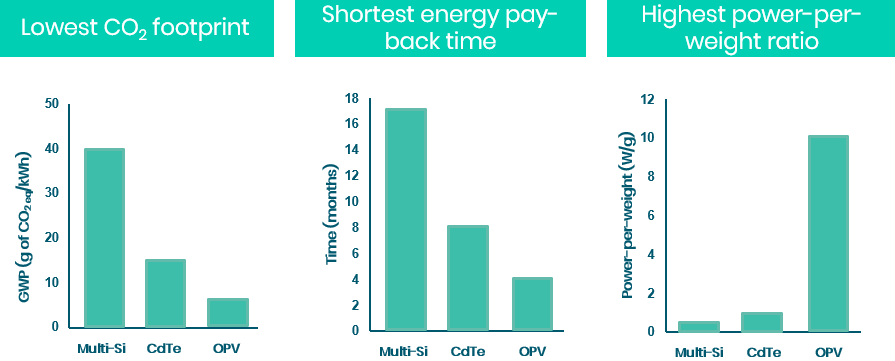
Also, with their flexible and lightweight properties, organic solar cells can be integrated into common objects, like backpacks, to recharge small electronic devices (i.e. cell phones and portable computers) while you walk to the office. Flexible organic photovoltaic devices are also the solar cells exhibiting the lowest CO2 footprint manufacturing, the lowest energy pay-back time (the time to produce the energy consumed for the fabrication of the solar cells) and the highest power-per weight ratio. Ajouter sources
At the end of the day, we can think of OPV as the transportable energy production source for day-to-day life at a fair price.
Figure 1: Difference in CO2 footprint, energy pay-back time and the power-per-weight ratio of OPV and more common photovoltaic devices.

As mentioned in the section of the semiconductor, the modulation of the organic semiconductor properties is a key component especially in OPV since they are the materials that will absorb the light to generate current.
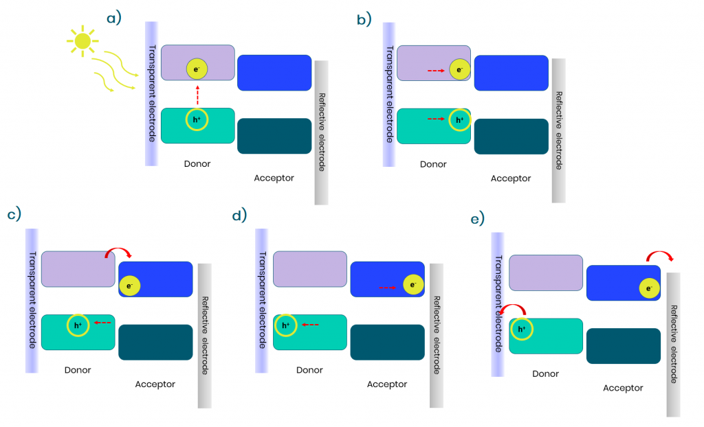
Organic solar cells are composed of two semiconducting materials, a donor and an acceptor. The bandgap of those materials plays a major role here. Indeed, when the solar cell will be illuminated, the photons emitted by the sun that possess higher energies (or lower wavelength) than the bandgap of the materials will be absorbed by the semiconductors to generate an exciton. This means that an electron from the valence band will be promoted to the conduction band creating a hole-electron pair. To be dissociated, the hole-electron pair must travel to the junction of the donor and acceptor phases which should be at a distance of about 10 to 20 nm. Then the charge dissociation, which is driven by the energy difference between the conduction band of the donor and the acceptor, will occur at the junction of both materials to create charge carriers that are no longer coulombically bounded. Those charges can then move in their respective phases to their respective electrode.
The donor and the acceptor organic semiconductors should possess complementary light absorption to cover the maximum of the solar emission spectrum. This is possible by designing materials with a carefully optimized bandgap, valence band (HOMO) and conduction band (LUMO).
Figure 2: different stage for the creation of current in an organic bulk-heterojunction solar cell a)Creation of an exciton b) migration of the exciton to the donor-acceptor junction c) charge dissociation d) charge transport to the electrodes e) charges are collected to their respective electrode

At Brilliant Matters, we produce a large catalog of the stat-of-the-art materials for both donor and acceptor materials. OPV is a booming technology where new materials emerge rapidly. With is experts’ teams Brilliant Matters is always on the first line for the production of these semiconductors with high quality, purity and reliability.

